Overview
The primary purpose of the circuit simulation is to provide students with a realistic environment where they can explore and better understand the concepts governing electronic circuits and their components. In the circuits laboratory, experiments are performed in a framework consistent with the other virtual labs; that is, students are put into a virtual environment where they are free to choose their objects and equipment, build a conceptual experiment of their own design, and then experience the resulting consequences. The focus in the circuit simulation is to allow students the flexibility to perform fundamental circuit experiments with a wide variety of components to teach the basic concepts of electronics and circuits that are easier to model in a simulated environment rather than a real laboratory. The important principles, features, and assumptions forming the foundation of the circuit simulation are listed below.
- The simulation uses a typical breadboard consisting of two independent sections each with its own power strip. Components inserted into each pin are assumed to make a perfect connection resulting in no loss of power or contact resistance.
Resistors, light bulbs, capacitors, inductors, a battery, and a function generator are the allowed components. These can be connected together in series, parallel, and any other combination on the breadboard, or on the schematic. Only one power source can be applied to the circuit.
Resistors can be ideal or non-ideal. Ideal means it has a perfect resistance or the stated value of the resistor is the actual resistance. For non-ideal or real resistors a tolerance can be set such that the value of the resistance is randomly assigned to be within a certain chosen range as occurs for real resistors. The actual value of the resistance will need to be measured since only its nominal value will be displayed.
Wires can be either ideal or non-ideal. Ideal means they connect the nodes and contribute no resistance to the circuit. Non-ideal means they are assumed to have some small resistance as every real wire does. This resistance is set randomly between a minimum and maximum value.
Square wave and saw tooth wave forms from the function generator are by necessity represented by rather short power series and will not be smooth. In addition, neither of those wave forms will work at high frequencies and my cause the simulation to hang.
The RMS voltage and current values for AC circuits measured with the Digital Multimeter (DMM) are calculated as an appropriate root-mean-square running sum. Consequently, the RMS values may not be exact especially at low frequencies.
- When the DMM is attached to a circuit and the DMM is set to measure resistance, the following will occur: (a) If the battery or function generator is attached to the circuit and is on, then the measured resistance on the DMM will be random since the current from the battery or function generator will interfere with the measurement. (b) If the battery or function generator is attached to the circuit but off, then it will act as if it has an infinite impedance. (c) If the circuit contains a capacitor, then the capacitor is treated as an open in the circuit. (d) If the circuit contains an inductor, then the inductor is treated as a short in the circuit.
Capacitors can be charged and discharged, however a capacitor will discharge if it is moved while it is charged and it may also discharge if the circuit is changed significantly.
Resistors are power limited and will burn out if their power rating is exceeded. Note that there is an approximate 10-second delay before the resistor burns when the power limit is exceeded.
The battery and DC source on the function generator is actually an extremely long time period sine wave at its maximum amplitude.
The DMM uses the nodal voltages of the circuit to determine the “measured” voltage of the selected part of the circuit. It also uses a 1 mA current for the resistance measurement.
The nominal resistance of a light bulb is calculated assuming 120 VAC is applied or 84.78 VRMS. Using this resistance, light bulbs are treated like resistors and the brightness of the light bulb is a linear function of the power dissipated across the resistive element. Light bulbs are considered to be everlasting meaning they can only blow out when they exceed their current threshold but they will not wear down. The filaments are considered to be perfect with no impurities to cause hotspots.
We transform all components into the Laplace domain then use a generalized nodal analysis to calculate the nodal voltages. From these voltages we can compute currents and impedances and then transform back to the time domain using inverse Laplace techniques.
The battery and function generator are perfect output devices with an infinite output impedance and no current limit.
Simulation Equations
Overview
The principal equations governing the calculation of a circuit are Ohm’s Law, V = i ∙ R, where V is the voltage, i is the current, and R is the resistance, and Kirchoff’s Laws. The method we chose to perform a generalized and complete analysis of a circuit was to transform the problem into the Laplace domain. The passive components, which is what we limit ourselves to in this simulation, can be easily transformed into the Laplace domain and then we perform a generalized nodal analysis using Gaussian Elimination with backwards substitution to solve for the nodal voltages. We then use an inverse Laplace algorithm to transform back to the time domain using a partial fraction expansion. For all calculations we solve the circuit in the Laplace domain and then transform the answer or resulting Laplace domain equation to the time domain.
We use the following Laplace transform components:
| Component | Time Domain | Laplace Domain |
| Resistors | R | R |
| Capacitors | C | 1 ∕ (C ∙ s) |
| Inductors | L | L ∙ s |
| DC | V0 | V0 ∕ s |
| Sine Wave | V0 ∙ sin(ω ∙ t) | V0 ∙ ω ∕ (s2 + ω2) |
Generalized Nodal Analysis
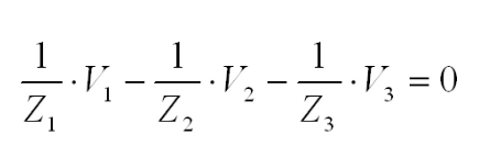
After the circuit is constructed on the breadboard we apply Kirchoff’s current law to generate a system of equations with the nodal voltages as the variables. Using the negative side of the power supply as a reference node, we can create a system of equations by balancing the current going into and out of each node. An example would look like the following for Node 2:
Then with the other equations for all the nodes you can use Gaussian Elimination to solve for the voltages. From these voltages we can then create the appropriate Laplace domain equation that represents the information being measured by the DMM or oscilloscope. The form of the Laplace equation is L(s) = N(s)/M(s) where N(s) and M(s) are polynomials of order kmax and jmax, respectively, and kmax must be less than jmax. The inverse Laplace transform is calculated using the following equation:
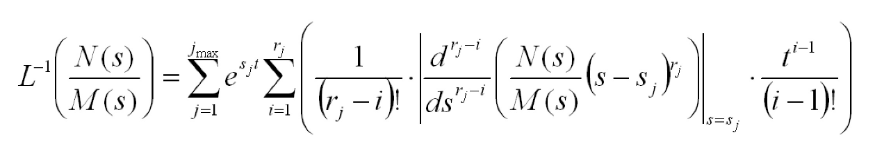
where sj is the jth root of M(s) with multiplicity rj.